本文档主要介绍板卡硬件接口资源以及设计注意事项等内容,测试板卡为创龙科技旗下的全志A40i+Logos FPGA开发板。
This document describes, among other things, the hardware interface resources of the card and the design attention, and tests the card for the A40i+Logos FPGA development board under the Dragon Technology flag.
核心板的ARM端和FPGA端的IO电平标准一般为3.3V,上拉电源一般不超过3.3V,当外接信号电平与IO电平不匹配时,中间需增加电平转换芯片或信号隔离芯片。按键或接口需考虑ESD设计,ESD器件选型时需注意结电容是否偏大,否则可能会影响到信号通信。
The ARM end and the IO level at the FPGA end of the core plate are generally 3.3V, and the power source is normally not more than 3.3V. When the external signal level does not match the IO level, the intermediate is required to add a level conversion chip or signal isolation chip. The key or interface needs to be considered for the ESD design, and the ESD device is selected in such a way as to be sensitive to the size of the capacitor, which may affect signal communication.
核心板CPU、ROM、RAM、电源、晶振等所有器件均采用国产工业级方案,国产化率100%。同时,评估底板大部分元器件亦采用国产工业级方案。
All core units such as CPU, ROM, RAM, power sources, crystals, etc. are in the national production industry programme, with a national production rate of 100%. At the same time, most components of the evaluation floor panels are in the national production industry programme.
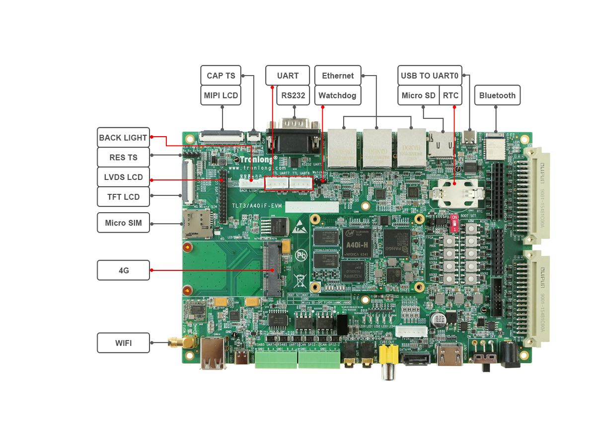
图 1 评估板硬件资源图解1
Figure 1 Chart of the assessment board hardware resources1
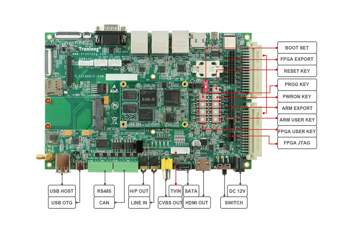
图 2 评估板硬件资源图解2
Figure 2 Evaluation board hardware resource diagram 2
CON13为MIPI LCD接口,采用40pin FFC连接器,间距0.5mm。
CON13 is a MIPI LCD interface with a 40pin FFC connector with a spacing of 0.5 mm.
J7为MIPI LCD的电容触摸接口CAP TS,采用6pin FFC连接器,间距0.5mm。
J7 is the capacitation touch interface CAP TS for MIPI LCD using a 6pin FFC connector with a spacing of 0.5 mm.
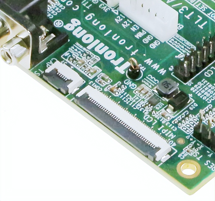
图 42
Figure 42
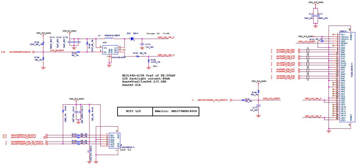
图 43
Figure 43
设计注意事项:
Design attention:
(1)若CAP TS(J7)的nINT引脚需分配使用其他IO,请使用引脚信号名称包含EINTx字段(支持中断功能)的IO引脚。
(1) If the CAP TS(J7) nINT foot needs to be assigned to other IOs, use the reference signal name to include the IO in the EINTX field (support to interruption).
CON10为TFT LCD接口,采用40pin FFC连接器,间距0.5mm。
CON10 is a TFT LCD interface with a 40pin FFC connector with a spacing of 0.5 mm.
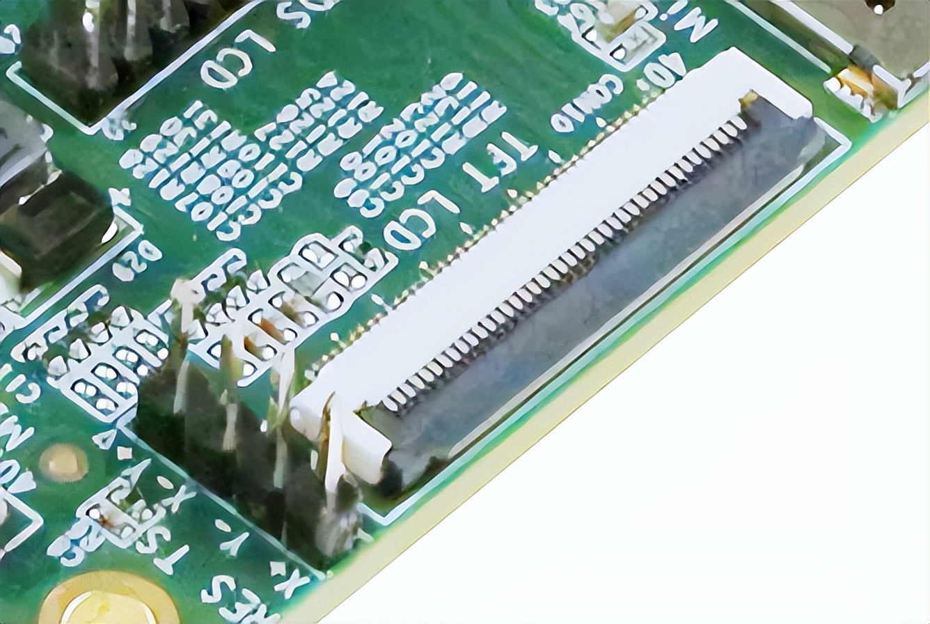
图 44
Figure 44
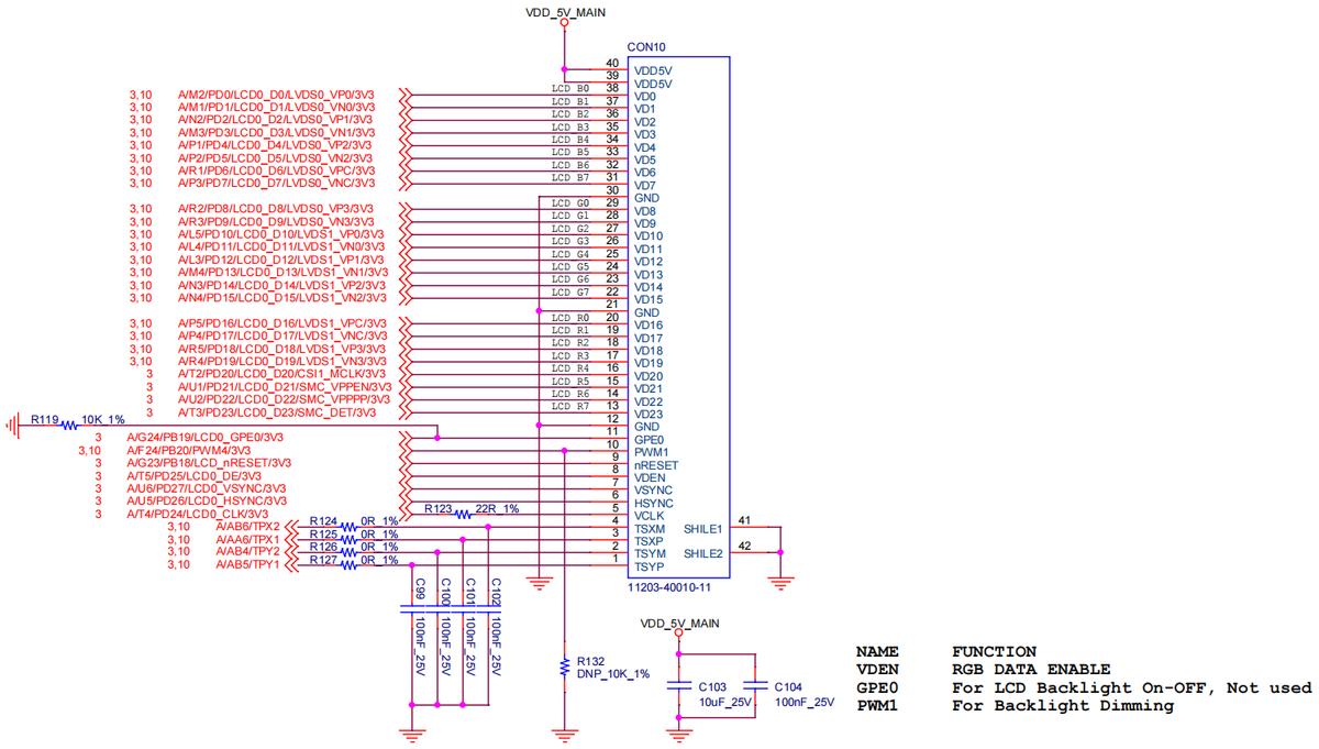
图 45
Figure 45
设计注意事项:
Design attention:
- TFT LCD接口使用的LCD0信号与LVDS0、LVDS1信号为复用关系,如下图所示。
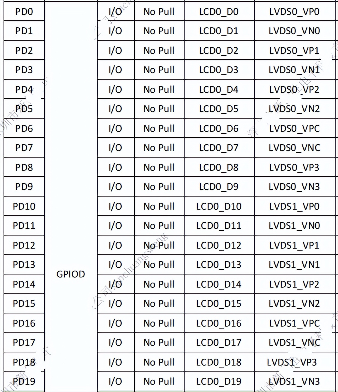
图 46
Figure 46
通过A/F24/PB20/PWM4/3V3引脚输出PWM控制LCD背光,外部预留下拉10K电阻到地。
PWM control of LCD backlights via A/F24/PB20/PWM4/3V3, leaving 10 K electric resistion outside.
TFT LCD接口、LVDS LCD接口已同时连接TPX1、TPX2、TPY1、TPY2四线电阻触摸信号,请勿同时连接两种显示设备。
The TFT LCD interface and the LVDS LCD interface have been connected to TPX1, TPX2, TPY1, TTPY2 four-line electrical resistance touch signals and do not connect to both display devices at the same time.
CON11为双路8bit LVDS LCD接口,采用2x 15pin双排针,间距2.0mm,包含LVDS信号及供电电源。CON12为背光控制接口,采用6pin白色端子座,间距2.54mm。J6为电阻触摸屏接口,采用4pin排针,间距2.54mm。
CON11 is a double-circuit 8bit LVDS LCD interface with 2x15pin double-drain needles with a distance of 2.0 mm, containing a LVDS signal and power supply. CON12 is a backlight control interface with 6pin white cognacs with a distance of 2.54 mm. J6 is an ETC screen interface with 4pin needles with a distance of 2.54 mm.
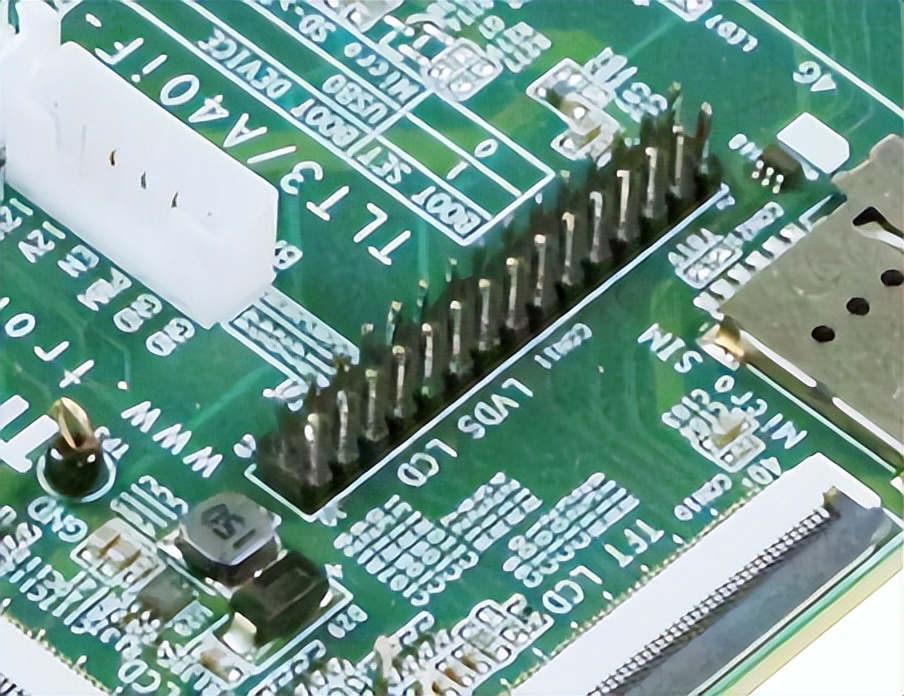
图 47
Figure 47
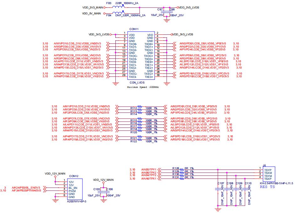
图 48
Figure 48
设计注意事项:
Design attention:
- LVDS0、LVDS1信号与LCD0信号为复用关系。
- LVDS LCD接口、TFT LCD接口同时连接了TPX1、TPX2、TPY1、TPY2四线电阻触摸信号,请勿同时连接两种显示设备。
CON9为HDMI OUT视频输出接口,采用标准19pin HDMI座。
CON9 is the HDMI OUT video output interface using standard 19pin HDMI.
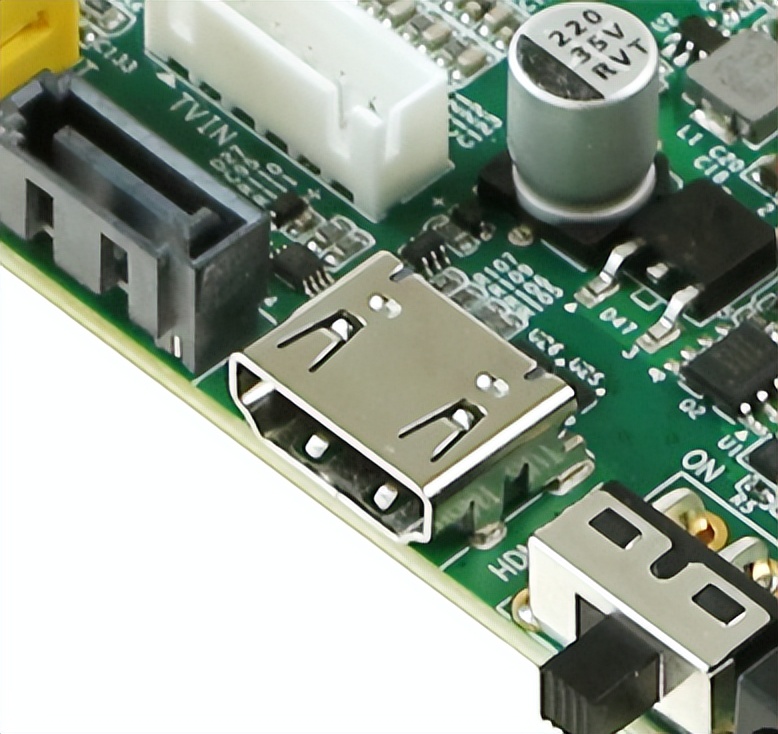
图 49
Figure 49
设计注意事项:
Design attention:
- HDMI座子的HPLG信号需下拉38.3K电阻到地,当外部设备接入时,会将此信号拉高。
- A/V9/HDMI_HSCL/3V3和A/W9/HDMI_HSDA/3V3的IO电平为3.3V,需转换为5V电平再引出至HDMI座。
J9为CVBS OUT接口,由TVOUT3引出,采用RCA莲花座。
J9 is the CVBS OUT interface, drawn from TVOUT3, using the RCA Lotus.
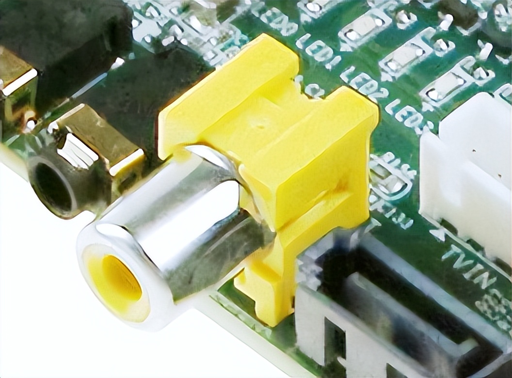
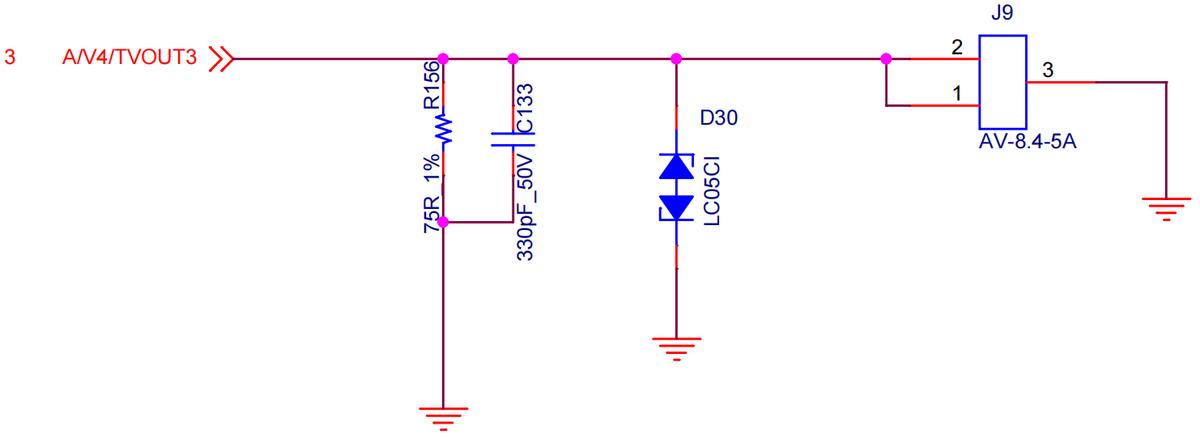
图 52
Figure 52
J8为TVIN接口,由TVIN0、TVIN1、TVIN2、TVIN3引出,采用6pin 2.54mm白色端子形式。
J8 is the TVIN interface, drawn from TVIN0, TVIN1, TVIN2, TVIN3, in the form of a white pin 2.44 mm.
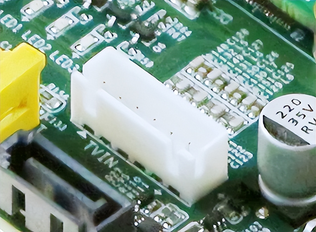
图 53
Figure 53

图 54
Figure 54
CON16(USB1 HOST)为USB2.0 HOST接口,采用双层Type-A型连接器;CON17(USB0 OTG)为USB2.0 OTG接口,采用Type-C连接器。
CON16 (USB1 HOST) is a USB 2.0 HOST interface using a double-story Type Type Type Type Type Type Type Type-A connector; and CON17 (USB0 OTG) is a USB 2.0 OTG interface using a Type-C interface.
评估底板通过USB HUB芯片将USB1总线拓展为4路USB HOST总线,将其中2路引出至USB1 HOST接口。
The evaluation base plate expanded the USB1 bus through the USB HUB chip to USB HIST 4 and led two of the routes out to the USB1 HIST interface.
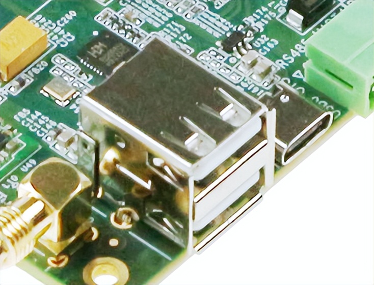
图 55
Figure 55
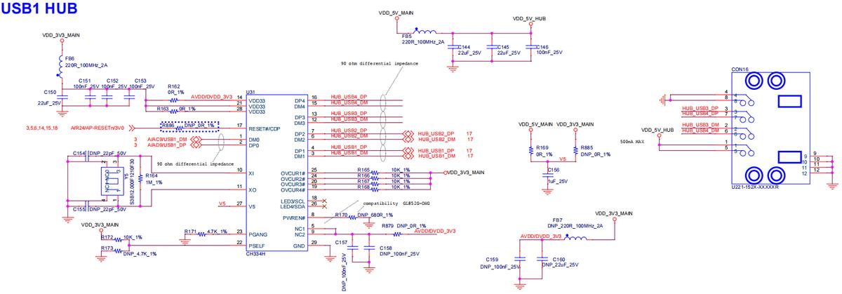
图 56
Figure 56
USB0 OTG接口直接由USB0总线引出。
The USB0 OTG interface is drawn directly from the USB0 bus.

图 57
Figure 57
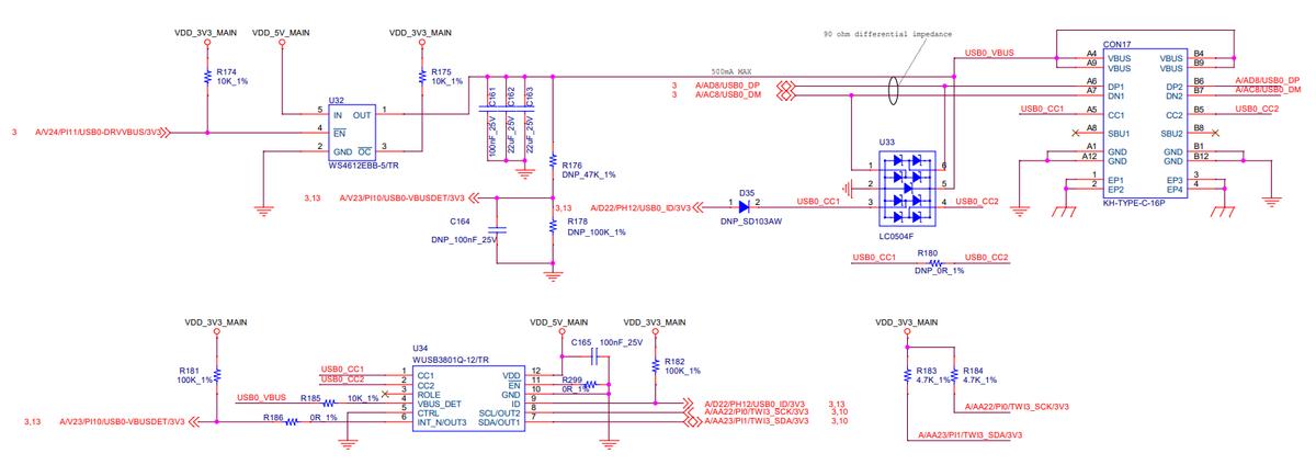
图 58
Figure 58
评估板包含1个ETH0 RGMII千兆网口、1个ETH1 MII百兆网口和1个ETH2 USB百兆网口。
The evaluation board consists of one ETH0 RGMII gigabytes, one ETH1 MII and one ETH2 USB.
CON18为ETH0 RGMII千兆网口,RJ45连接器已内置隔离变压器。
CON18 is the ETH0 RGMII gigabyte, and the RJ45 connector is built into the isolation transformer.
备注:A40i处理器内部集成1个GMAC控制器,支持1路RGMII千兆网口。
Note: The A40i processor is internally integrated into a GMAC controller supporting the 1-way RGMII gigabytes.
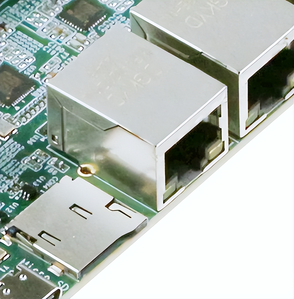
图 59
Figure 59
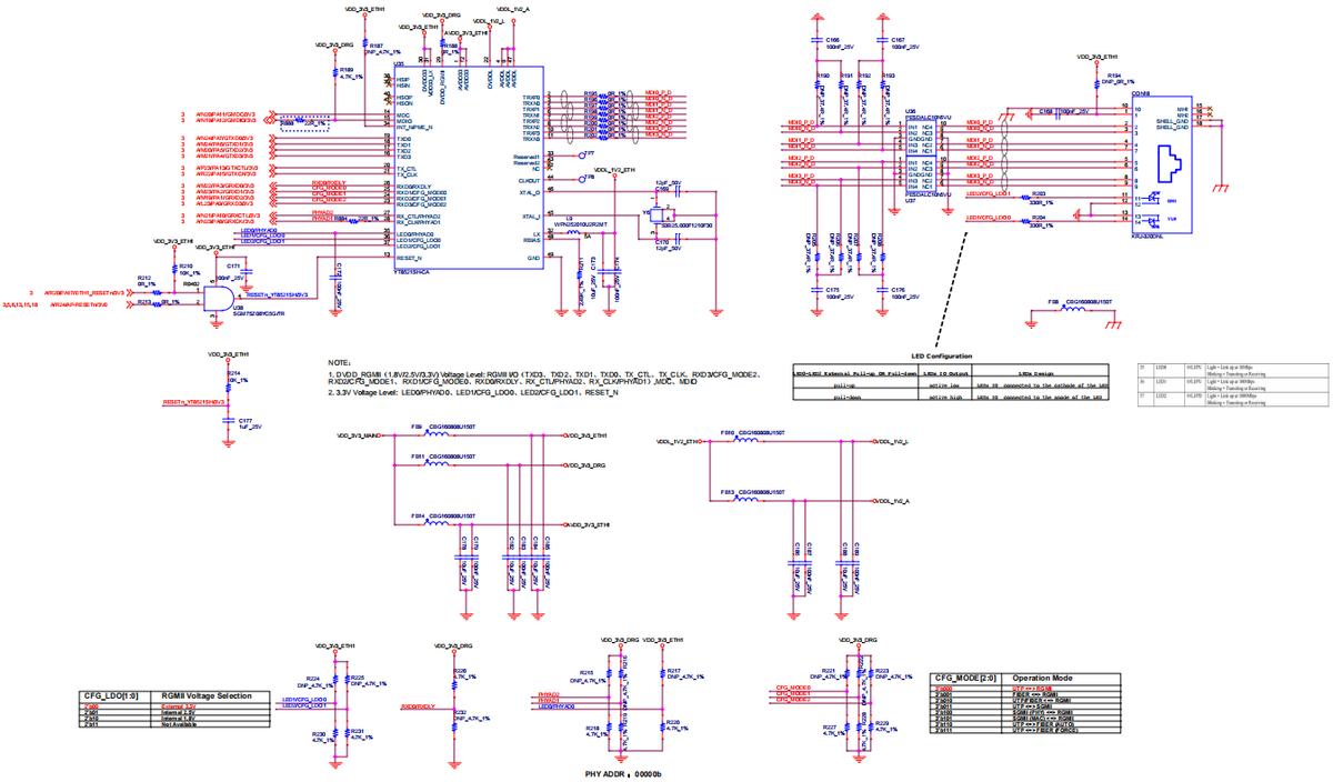
图 60
Figure 60
设计注意事项:
Design attention:
- VDDL_1V2_ETH电源为YT8521SH-CA内部输出,请勿用于其它负载供电。
- XTAL_I、XTAL_O引脚接入25MHz无源晶振。如需使用25MHz有源晶振,可从XTAL_I引脚接入,XTAL_O引脚悬空处理。
- YT8521SH-CA芯片要求在供电稳定后,保持10ms后再拉高复位信号。请参考评估底板的复位电路方案,使用IO控制网口复位。
- YT8521SH-CA芯片管脚LED0/PHYAD0、LED1/CFG_LDO0、LED2/CFG_LDO1、RESET_N的信号电平皆为3.3V,上拉配置时,请上拉到3.3V;其他信号管脚上拉配置时,请上拉到DVDD_RGMII(1.8V/2.5V/3.3V)电源。

图 61
Figure 61
CON19为ETH1 MII百兆网口,采用RJ45连接器,已内置隔离变压器。
CON19 is the ETH1 MII 100-millimeter portal, using RJ45 connectors, and has built-in isolation transformers.
备注:A40i处理器内部集成1个EMAC控制器,支持1路MII百兆网口。
Note: The A40i processor is internally integrated into an EMAC controller to support the MII 100-millimeter portal on route 1.
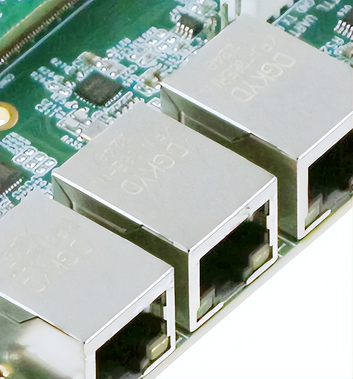
图 62
Figure 62

图 63
Figure 63
设计注意事项:
Design attention:
- XTAL_IN、XTAL_OUT引脚接入25MHz无源晶振。如需使用25MHz有源晶振,可从XTAL_IN引脚接入,XTAL_OUT引脚悬空处理。
- YT8512H芯片要求在供电稳定后,保持10ms后再拉高复位信号。请参考评估底板的复位电路方案,使用IO控制网口复位。
CON20为ETH2 USB百兆网口,采用RJ45连接器,已内置隔离变压器。
CON20 is the ETH2 USB 100-millimeter portal, with RJ45 connectors and built-in isolation transformers.
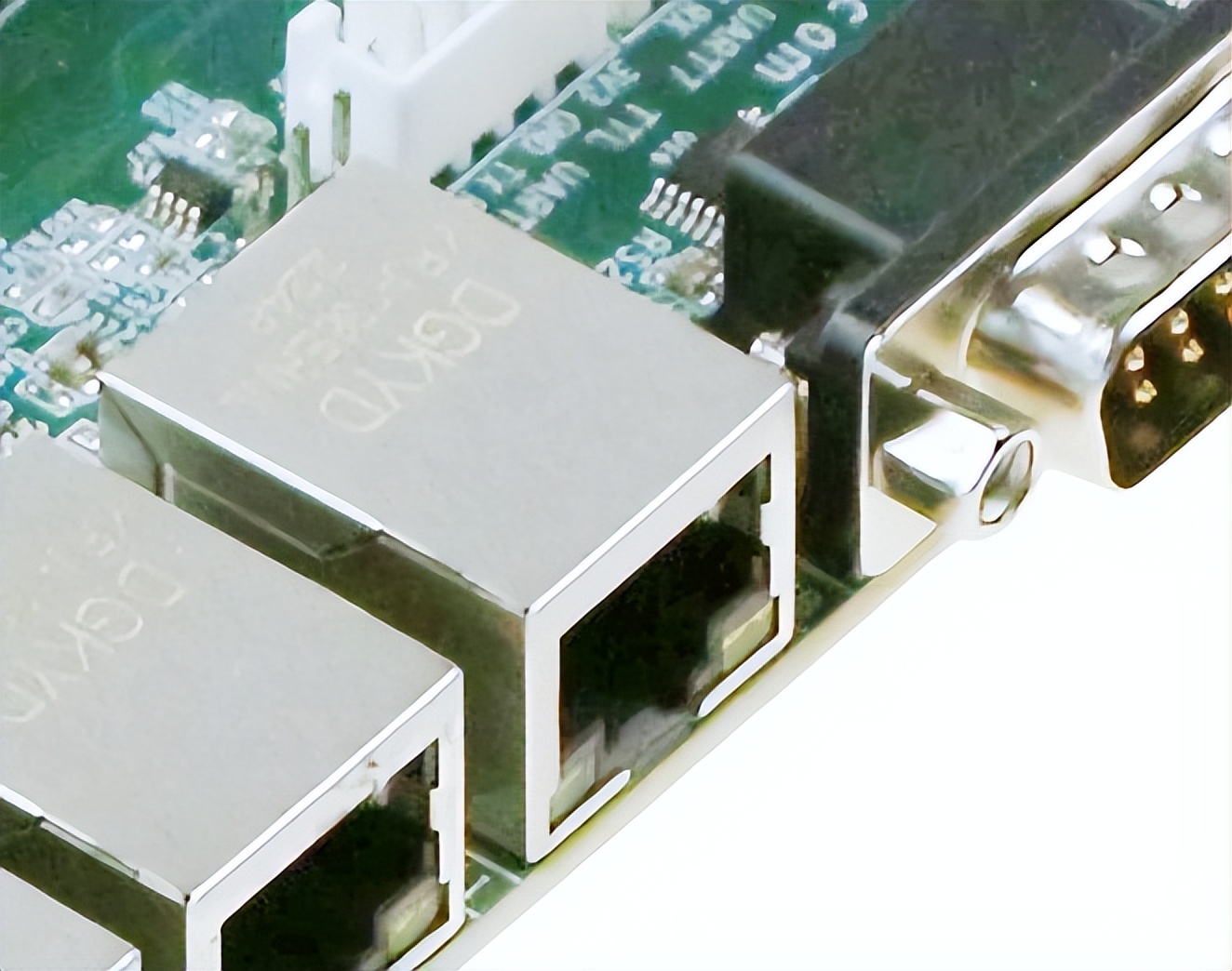
图 64
Figure 64
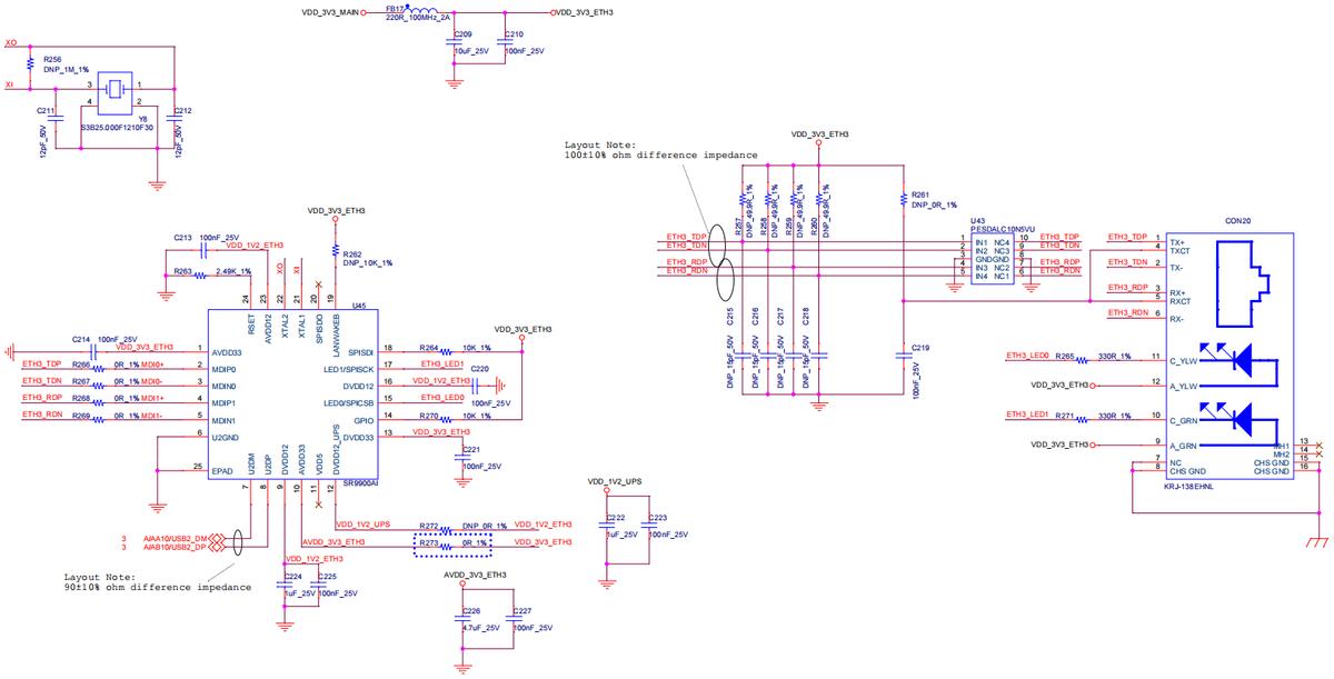
图 65
Figure 65
CON23为4G模块拓展接口,采用Mini PCIe插槽。评估底板通过USB HUB芯片将USB1总线拓展为4路USB HOST总线,其中引出一路进行4G模块拓展。
CON23 expands the interface for the 4G module using the Mini PCIe slot. The evaluation base plate expands the USB1 bus to USB HIST 4 through the USB HUB chip, which leads to a 4G module expansion.
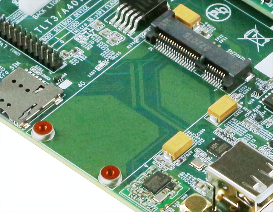
图 66
Figure 66
CON21为Micro SIM卡座,采用插卡自弹形式,不带检测引脚。
CON21 is Micro SIM, which is self-propelled in the form of a plug-in card and is not subject to detection.
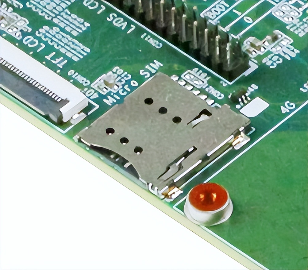
图 67
Figure 67
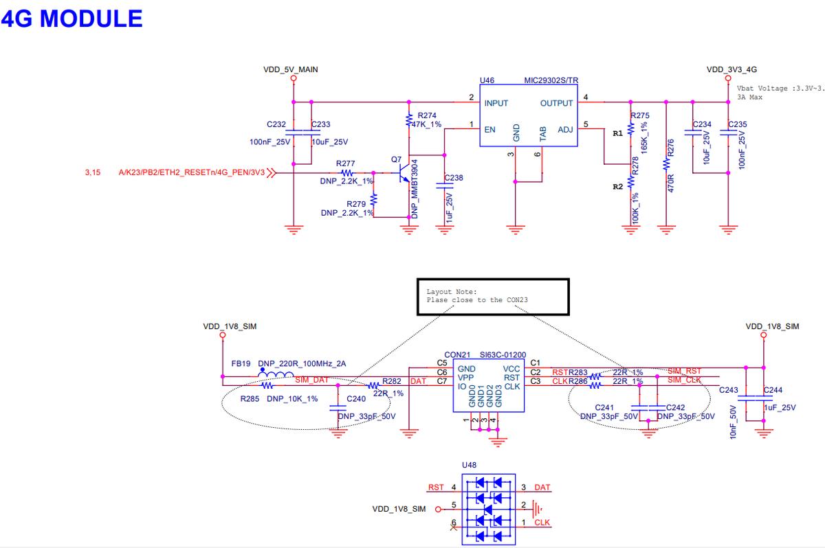
图 68
Figure 68
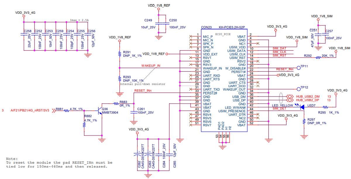
图 69
Figure 69
设计注意事项:
Design attention:
- 为保证4G模块有稳定的电源供应,其3.3V电源需由MIC29302S/TR(U46)独立供电,至少提供2A电流输出。如要替换其他电源,建议使用LDO,详细请参考4G模块数据手册要求。
- 如需控制4G模块供电,可贴上R277、R279电阻和Q7三极管,通过GPIO来控制4G模块电源使能状态。
评估底板通过USB HUB芯片将USB1总线拓展为4路USB HOST总线,其中引出一路进行WIFI模块拓展。板载WIFI模块(U49)型号为:必联BL-R8188EU2,采用邮票孔连接方式。
The evaluation base plate expands the USB1 bus to a 4-circuit USB HIST bus via USB HUB chip, which leads to an extension of the WIFI module. The model of the WIFI module (U49) is BL-R8188EU2, using a stamp hole connection.
备注:WIFI模块芯片生产商为台系厂家。
Note: The producer of the WIFI module chip is a plant.
CON22为SMA接口,用于外接WIFI模块的2.4G天线。
CON22 is the SMA interface for the 2.4G antenna attached to the WIFI module.
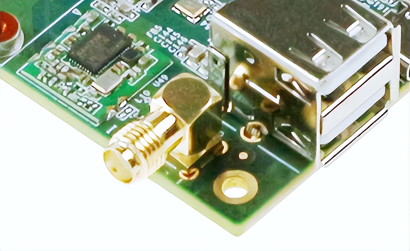
图 70
Figure 70
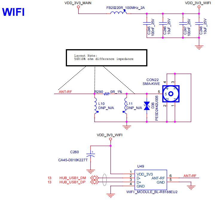
图 71
Figure 71
U47为板载蓝牙模块,通过UART2进行蓝牙模块拓展。型号为:亿佰特E104-BT5011A,采用邮票孔连接方式。模块自带PCB板载天线,无需外接天线。
U47 is a bluetooth module, which is expanded through UART2. The model is E104-BT5011A, with a stamp hole connection. The module carries an antenna with itself a PCB panel, without the need for an outside antenna.
备注:蓝牙模块芯片生产商为挪威厂家。
Note: Bluetooth module chip producers are Norwegian manufacturers.
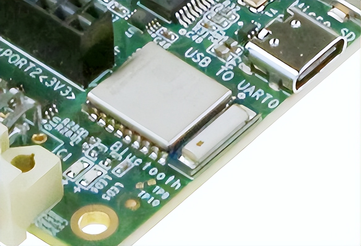
图 72
Figure 72
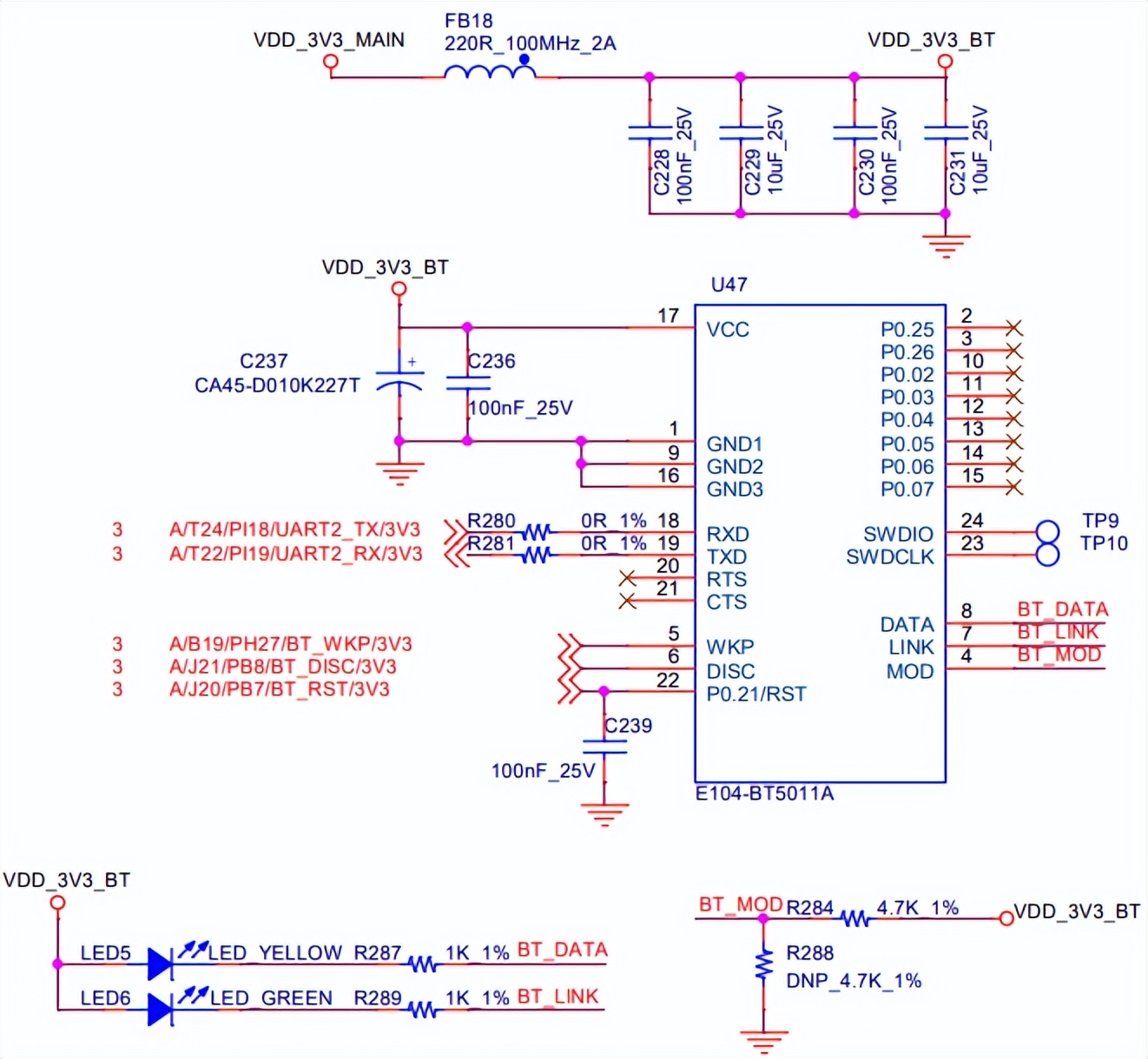
图 73
Figure 73
J4为标准7pin SATA硬盘接口。
J4 is a standard 7pin SATA hard disk interface.
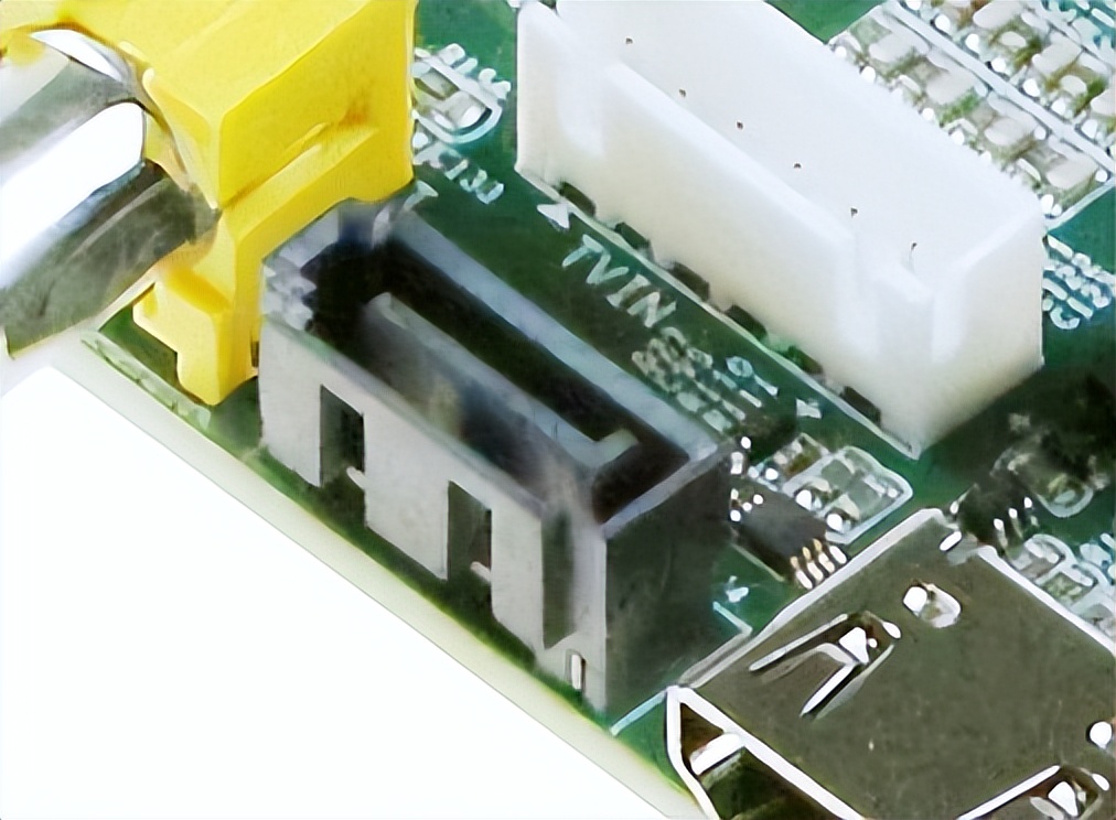
图 74
Figure 74
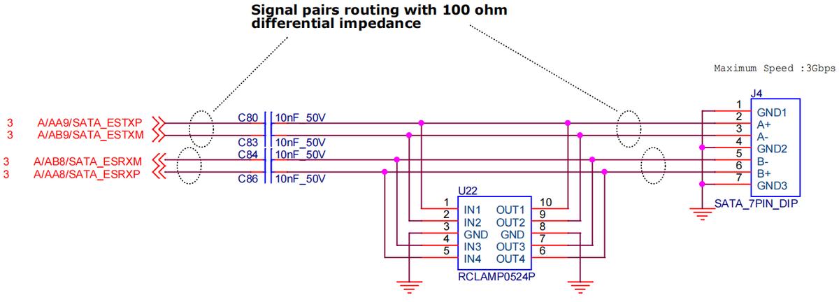
图 75
Figure 75
设计注意事项:
Design attention:
- SATA_ESTXP/M和SATA_ESRXP/M线路需靠近J4放置10nF的AC耦合电容。
CON5为FPGA JTAG仿真调试接口,采用14pin简易牛角座连接器,间距2.0mm,可适配创龙科技的TL-PGMCable下载器。
CON5 is a FPGA JTAG simulation interface using a 14pin Simple Bull Horner connector with a distance of 2.0 mm, a TL-PGCable downloader that can be adapted to the pioneer technology.
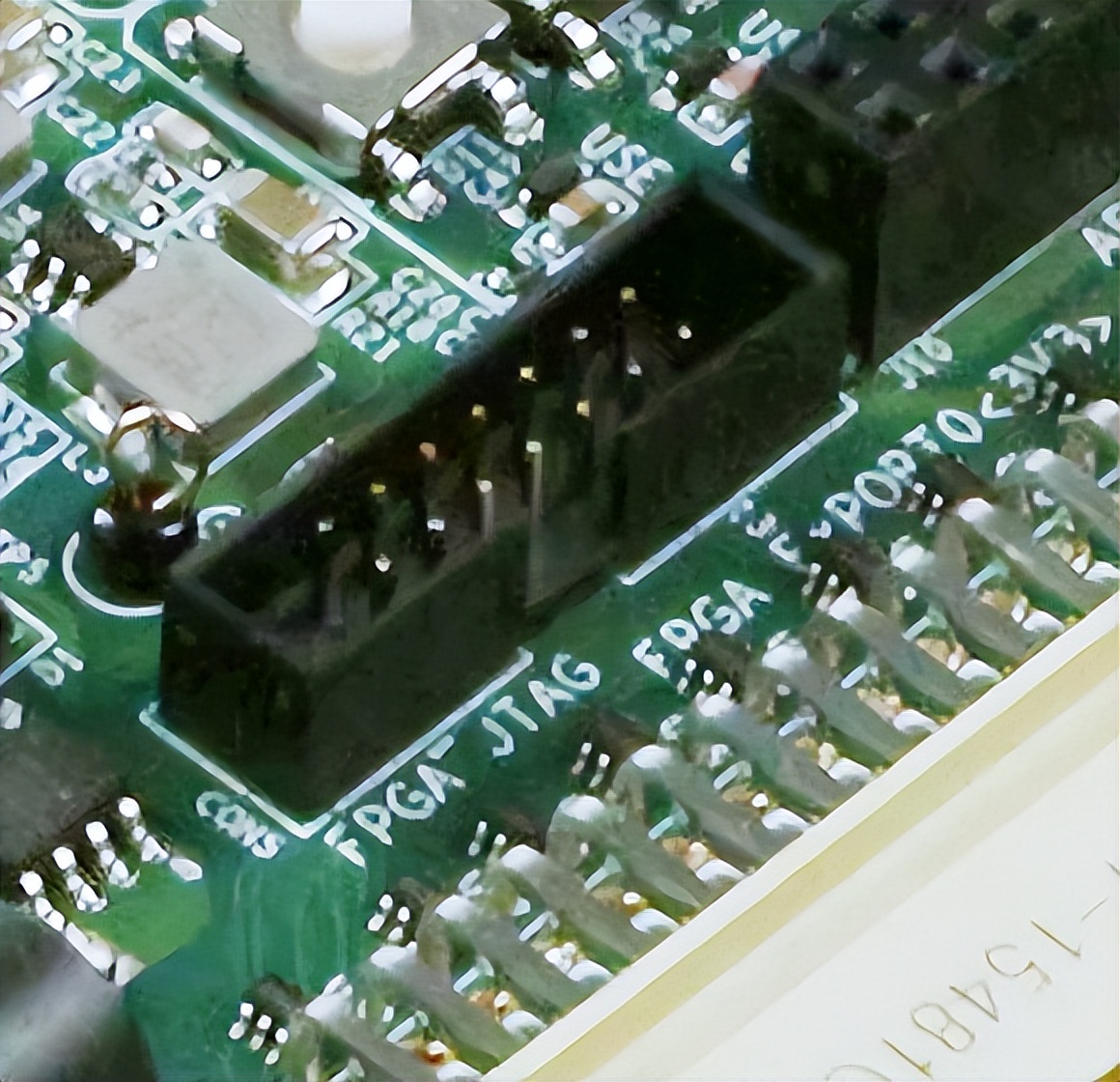
图 76
Figure 76
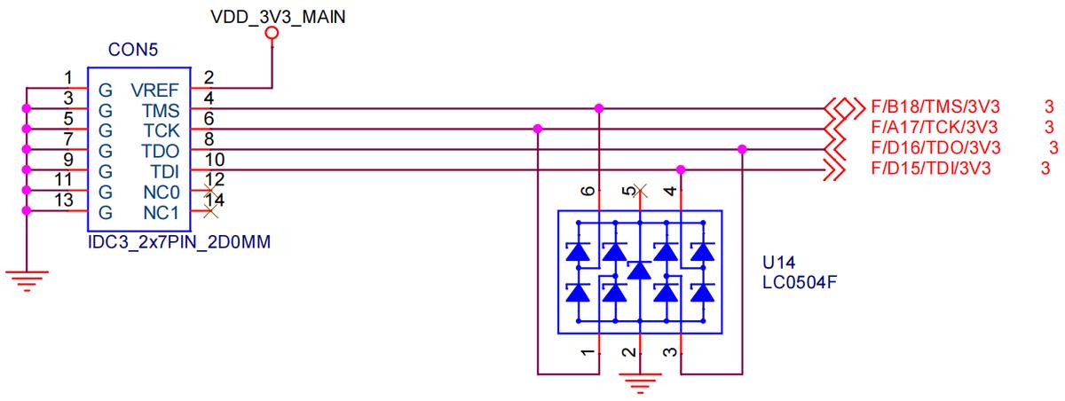
图 77
Figure 77
SDIO总线在核心板已用作ARM端与FPGA端的通信,在底板上不作为外设。
The SDIO bus has been used on the core plate as communication at the ARM end with the FPGA end and is not extrapolated on the base plate.

图 78
Figure 78
J10为ARM ExPORT0接口,采用2x 10pin排母,间距2.54mm,引出SYS_RESETn、AP-NMIn、Audio Codec、GPIO等拓展信号。
J10 is the ARM ExPORT0 interface, using 2x10pin platoon masters with 2.54 mm spacing, which leads to extended signals such as SYS_RESETN, AP-NMIn, Audio Codec, GPIO, etc.
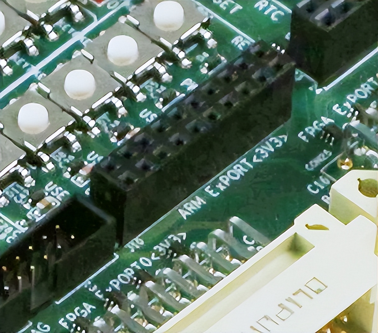
图 79
Figure 79
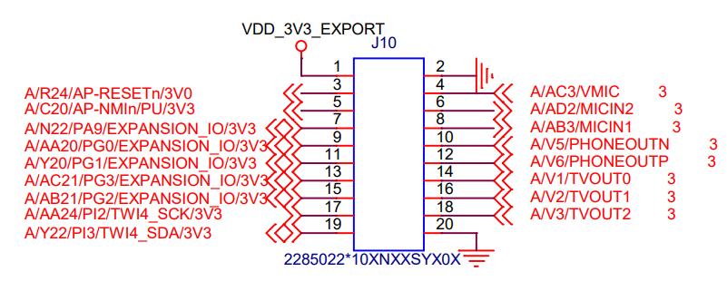
图 80
Figure 80
J11为FPGA ExPORT1接口,采用2x 12pin排母,间距2.54mm,引出FPGA端的IO拓展信号。
J11 is the FPGA ExPORT1 interface, using 2x12pin platoon mothers with 2.54 mm spacing, which leads to an IO extension signal at the FPGA end.
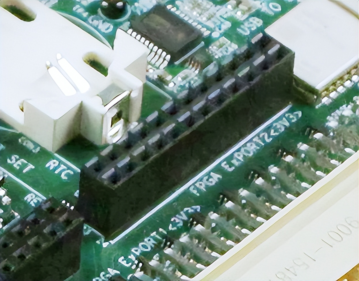
图 81
Figure 81

图 82
Figure 82
CON24和CON25为3x 16pin欧式端子公座,间距2.54mm,引出FPGA端的IO拓展信号。
Con24 and CON25 are 3x16pin European Portraits with 2.54 mm spacing, which leads to an IO extension signal at the FPGA end.
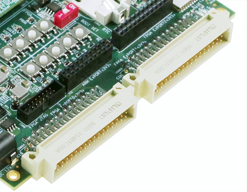
图 83
Figure 83
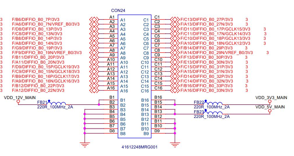
图 84
Figure 84
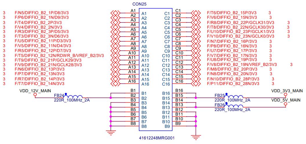
图 85
Figure 85
注册有任何问题请添加 微信:MVIP619 拉你进入群

打开微信扫一扫
添加客服
进入交流群


发表评论